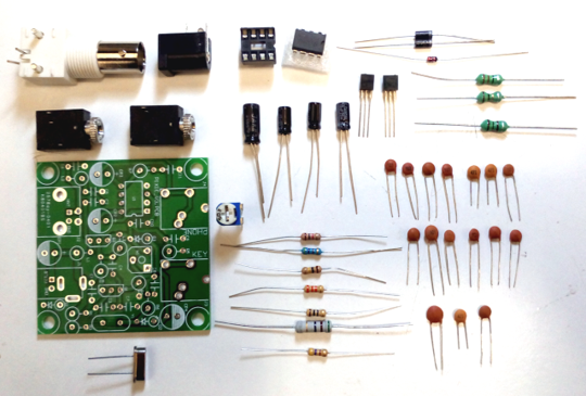
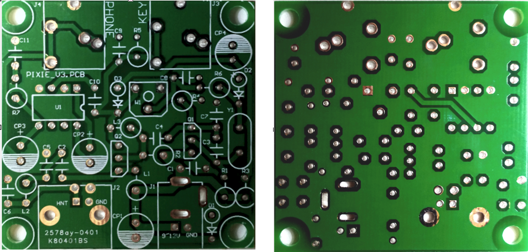
With the theory behind us, it is time to move to practice: physically assembling the Pixie. In this page we will see how to identify the kit components, how to inspect the printed circuit board before starting, and how to perform reliable soldering.
The kit components
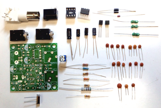
A typical Pixie kit includes: the printed circuit board (PCB), connectors (BNC for the antenna, jacks for the key and headphones), an IC socket, resistors, ceramic and electrolytic capacitors, two transistors, a diode, a crystal and a trimmer. Before starting soldering, it is always a good idea to make an inventory of everything received, comparing it with the bill of materials (BOM) supplied with the kit: it is much easier to identify a missing component at this stage than when the assembly is almost complete. It is also useful to mark the components already identified with a pencil or a check mark on the BOM, avoiding confusion between apparently similar parts.
The printed circuit board
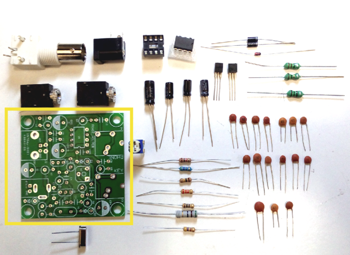
The printed circuit board (PCB) is the base on which all components will be soldered: the copper tracks printed on the surface provide the electrical connections defined by the schematic, replacing the point-to-point wiring used in older constructions.
Connectors
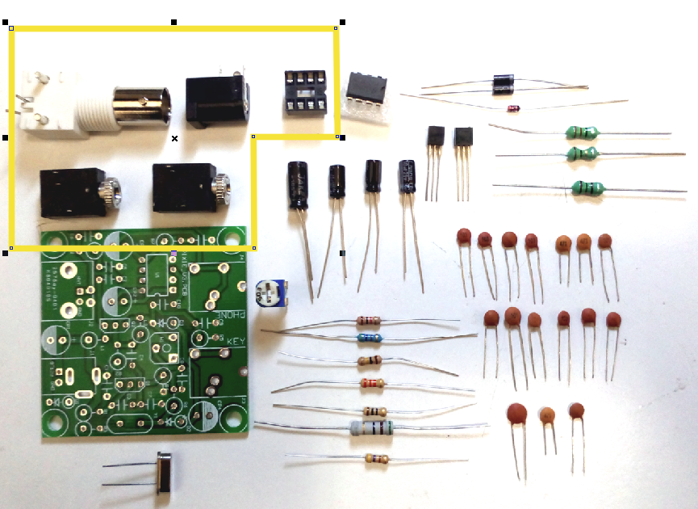
The connectors include the BNC connector for the antenna and the two jacks (for the Morse key and the headphones). The socket for the LM386 integrated circuit is optional, but recommended: it allows the IC to be replaced without desoldering it, in case of failure or assembly mistakes.
Passive components
Applying what we learned in the page about passive components, it is now time to identify, one by one, the value and type of each resistor (through the colour code), inductor and ceramic capacitor (through the printed marking), comparing them with the schematic. I suggest soldering the components afterwards in this order. For diodes and electrolytic capacitors it is essential to correctly identify the orientation, since they have a mandatory polarity.
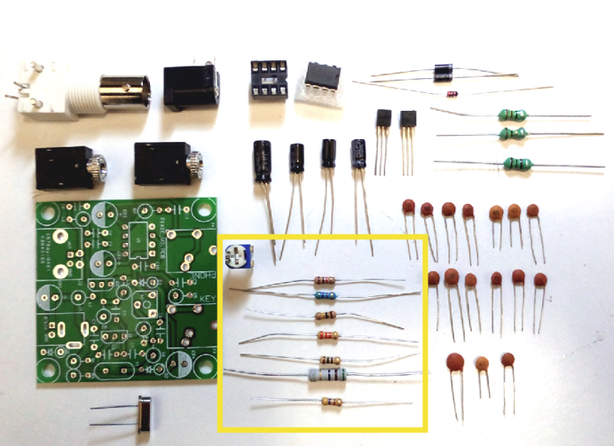 Resistors |
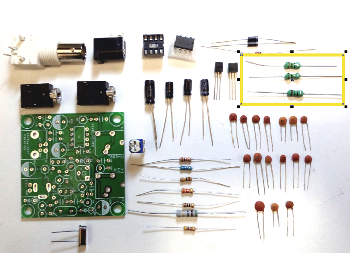 Inductors |
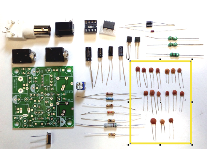 Ceramic capacitors |
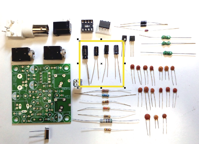 Electrolytic capacitors |
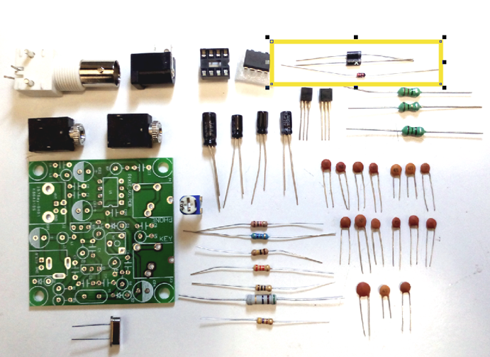 Diodes |
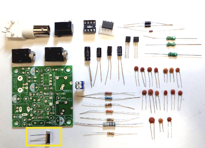 Crystal |
Active components
For these components as well, in addition to the value, it is essential to correctly identify the orientation. It is also necessary to pay greater attention to avoiding overheating the component during assembly, since excessive heat can seriously damage them. Remember that the two transistors are not interchangeable, and even if they may look identical externally, they can have different electrical characteristics and pin configurations.
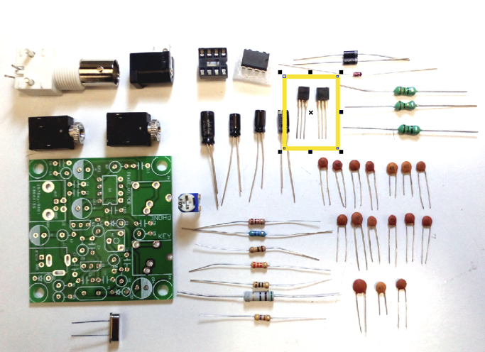 Transistors |
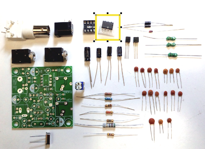 Integrated circuit |
Pay attention to the printed circuit board
Before installing the components, it is useful to carefully inspect the printed circuit board. In particular:
- if a hole is used to connect more than one track (plated through holes, vias), verify that the plating is intact and continuous between the two sides;
- it is necessary to visually follow the tracks to exclude the presence of copper burrs that could create unwanted short circuits, especially on inexpensive or lower-quality printed circuit boards.
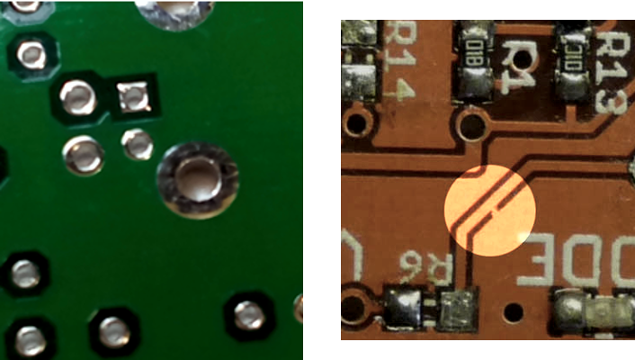
A few minutes spent on this preliminary inspection can save hours of troubleshooting once the assembly is complete.
Pay attention to component orientation
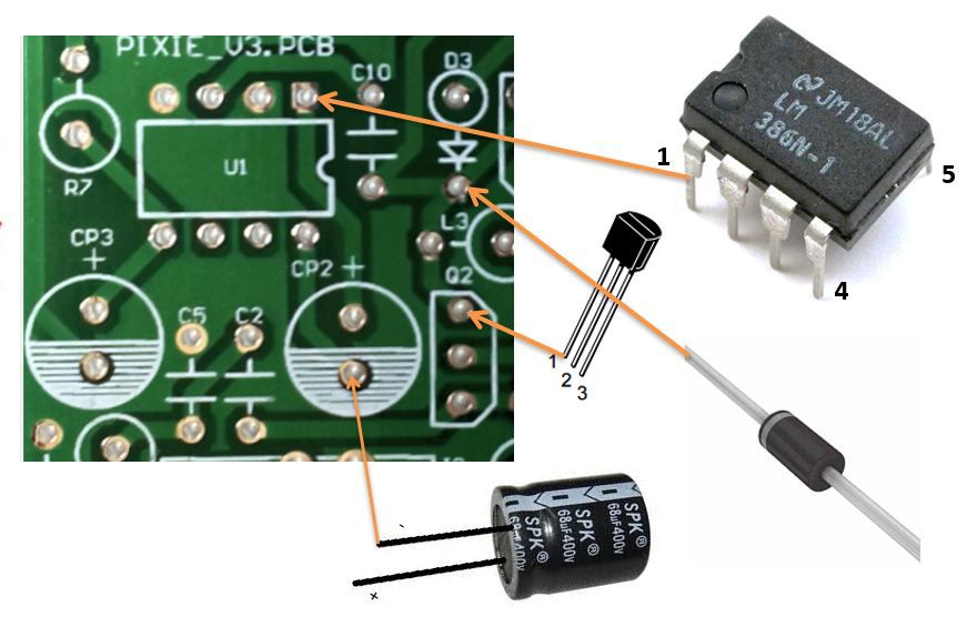
As mentioned earlier, several components have a mandatory mounting orientation, and the printed circuit board usually includes graphic indications (a stripe, a semicircle, a dot) to guide the correct assembly:
- the diode must be oriented according to the ring printed on its body, which indicates the cathode;
- the transistor has a specific pinout (base, collector, emitter) which may differ between transistor models and must match the outline printed on the PCB;
- the electrolytic capacitor has its negative terminal marked by a stripe on the body, which must match the indication on the PCB;
- the integrated circuit (LM386) has a reference mark (a notch or a dot) corresponding to pin 1, which must be aligned with the marking on the PCB.
An orientation mistake, as already discussed when describing individual components, is one of the most common errors, but it is also one of the easiest to avoid with a careful check before soldering.
Soldering technique
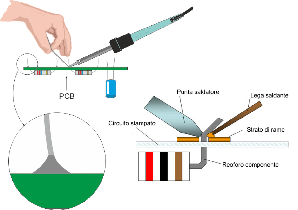
A good solder joint is obtained by following a precise sequence:
- heat simultaneously both the copper pad on the PCB and the component lead, keeping the soldering iron tip in contact with both;
- only after a short moment, bring the solder wire to the junction point (not directly to the soldering iron tip);
- the solder melts and spreads by capillary action around the lead, bonding both to the PCB copper and to the component terminal;
- remove the solder wire first, then the soldering iron, allowing the joint to cool without moving the component.
Recognizing a good solder joint
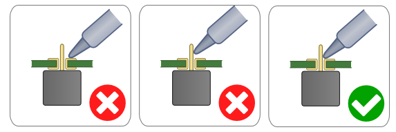
A properly made solder joint has a shiny appearance and a regular “cone” shape, surrounding the terminal without forming drops or irregular spikes. The most common defects to recognize and avoid are:
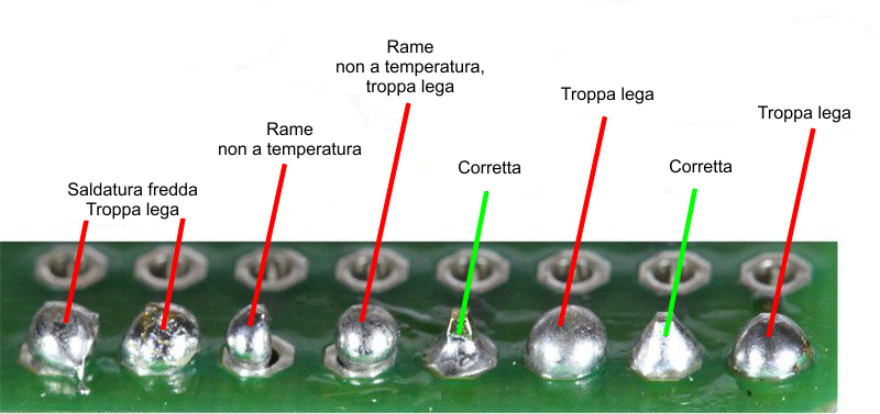
- cold solder joint: dull in appearance, often with a rough surface; it is caused by insufficient temperature or by moving the component while the solder is cooling;
- copper pad not heated enough: the solder does not spread correctly over the pad, remaining as a “ball” around only the component lead;
- too much solder: excess solder forming a protruding blob, aesthetically incorrect and potentially causing short circuits with nearby tracks.
The correct solder joint is the one that, with the minimum amount of solder required, forms a regular cone and adheres well both to the component and to the PCB pad.
Cleaning the soldering iron tip
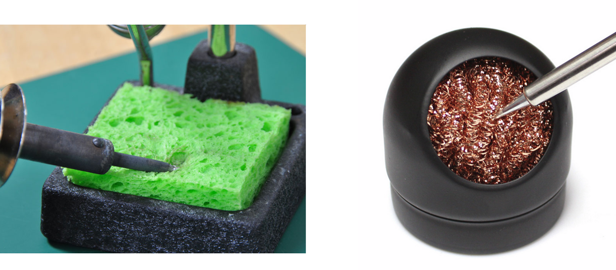
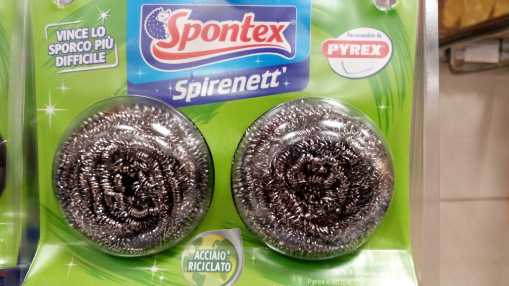
A clean tip is essential for reliable soldering. The most common methods are two: wiping the hot tip on a damp sponge, or — a more effective and less “traumatic” solution for the tip — on a small coil of brass wool. Material available in ordinary household stores can also be used, but it must be handled carefully because steel wool could damage soldering iron tips.
A note about soldering paste
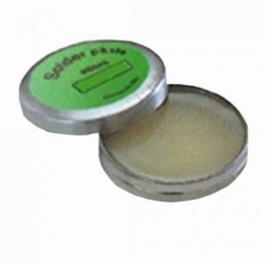
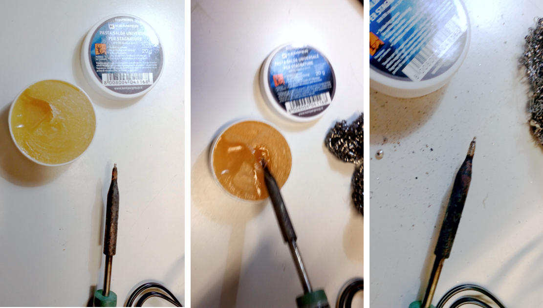
Traditional soldering paste is a mixture of resins and aggressive agents, traditionally used in plumbing or metalwork. It must never be used on printed circuit boards or, in general, in electronics: it triggers corrosive processes that, over time, cause damage that is often not immediately visible but can nevertheless be serious.
Modern solder pastes, specifically formulated for electronic use, can instead be used carefully to refresh oxidized soldering iron tips, but this is a completely different application from actual soldering.
Flux, on the other hand, is a chemical compound specifically designed to facilitate the flow of molten solder and prevent oxidation during the soldering process: it allows uniform distribution and removes the light oxidation present on leads and pads without damaging delicate parts.
Essential tools
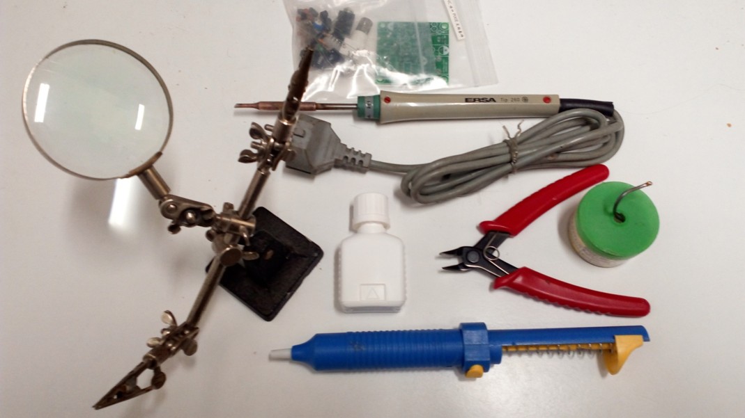
For a job like this, in addition to the soldering iron, the following tools are very useful:
- a magnifying glass, preferably integrated into a “third hand” holder, which keeps the PCB steady during soldering;
- a solder sucker, to correct possible mistakes;
- a pair of side cutters to trim excess component leads after soldering;
- good quality solder wire, with an integrated flux core.
- flux, useful for difficult solder joints.
A multimeter is then absolutely indispensable.